What is a PCB Board and How is it Used in Electronics?
The Pcb Board, an essential component in modern electronics, plays a crucial role in circuit design and functionality. As per the IPC (Institute for Printed Circuits), the global market for PCB manufacturing was valued at approximately $61 billion in 2020 and is projected to reach about $80 billion by 2026. This growth reflects the increasing demand for electronic devices across various sectors, including consumer electronics, telecommunications, and automotive industries.
A PCB board serves as the backbone for electronic assemblies, providing mechanical support and electrical connections. Its design complexity varies widely, from simple single-layer boards to intricate multi-layer constructions. According to a report by Research and Markets, the demand for multilayer PCBs is expected to rise, driven by advancements in technology and miniaturization. However, despite these advancements, challenges remain in manufacturing processes and material selection.
Issues such as signal integrity and thermal management require ongoing research and expertise. PCB manufacturers must continually adapt to evolving industry standards. The importance of precise design and reliable materials cannot be overstated. A poorly designed PCB can lead to device failure, signaling the need for better practices in the field. The future of PCB technology will hinge on balancing innovation with reliability.
What is a PCB Board?
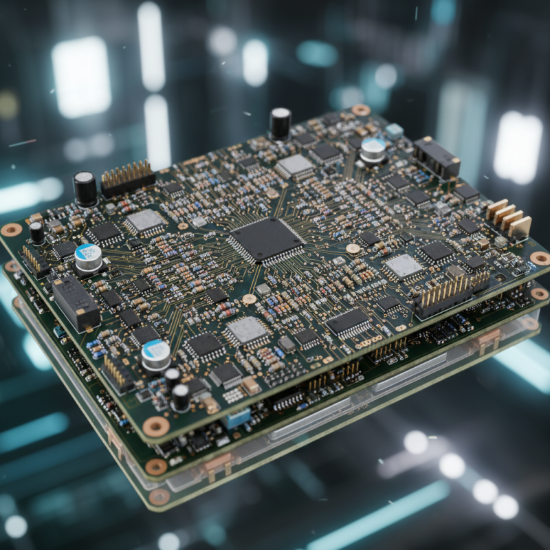
A PCB, or printed circuit board, is a crucial component in modern electronics. It serves as a foundation for connecting electronic components like resistors, capacitors, and microchips. In 2022, the global PCB market was valued at approximately $75 billion and is projected to grow steadily. This growth reflects the increasing demand for advanced electronic devices across various sectors.
The design of a PCB involves layering conductive pathways for electrons to flow. It can range from simple designs with few components to complex structures used in smartphones and computers. With the advancement in technology, many PCBs are now manufactured using eco-friendly processes, aligning with industry sustainability goals.
**Tips: Always consider the intended application when designing a PCB.** Precision in layout can significantly affect performance.
Errors in design or manufacturing can lead to circuit failures. It’s essential to conduct thorough testing. Data shows that up to 30% of PCBs face issues during production. Regular audits and checks can minimize these risks. **Tip: Utilize simulation software for better accuracy in designs.**
Key Components of a PCB Board
A PCB board, or printed circuit board, is vital in electronics. Its primary role is to connect electronic components. Understanding its key components is essential for anyone interested in engineering or electronics.
The board itself is made from insulating material, often fiberglass. This provides a sturdy base for the circuit. Conductive pathways, usually copper, are etched onto this board. These pathways form electrical connections between components. Common components include resistors, capacitors, and integrated circuits. Each serves a unique purpose, influencing how the entire circuit functions.
Tips: When designing a PCB, consider layout and space. An organized layout can prevent many issues during assembly. Additionally, ensure that the components selected fit within the board's design. This minimizes errors in functionality. Remember, testing is crucial. A small mistake can lead to significant problems later on.
What is a PCB Board and How is it Used in Electronics? - Key Components of a PCB Board
| Component | Description | Function | Material |
| Copper Traces | Conductive pathways | Connect electrical components | Copper |
| Silkscreen | Text and symbols printed on PCB | Mark component locations | Soldermask ink |
| Soldermask | Protective coating | Prevent solder shorts | Epoxy resin |
| Via | Plated holes | Connect layers in multilayer PCBs | Copper and dielectric material |
| Substrate | Base material of PCB | Support components and traces | FR4 (Fiberglass) |
Manufacturing Process of PCB Boards
The manufacturing process of PCB boards is intricate and requires precision. It typically begins with a base material. This base is often made from fiberglass, which provides strength. A thin layer of copper is then laminated on the substrate. This copper layer serves as the pathways for electrical signals.
Next, the design of the PCB is printed on this copper layer. This can be done using photographic films or direct printing methods. Afterward, unwanted copper is etched away. This process creates the necessary circuit patterns. The remaining copper is vital for the board's functionality.
Drilling holes for components follows the copper etching. Each hole allows for component leads to connect with the PCB, ensuring electrical continuity. Once drilling is done, a solder mask is applied. This mask protects the copper traces from damage. Additionally, silkscreen printing adds labels for better component identification. Each step must be executed carefully to avoid defects. Errors in any phase can impact the board's performance. This process highlights both the complexity and the necessity of quality control in PCB manufacturing.
Applications of PCB Boards in Electronics
PCB boards, or printed circuit boards, play a crucial role in the electronics industry. These boards serve as the foundation for various electronic devices. They connect different components and ensure they function properly. In modern devices, the complexity and miniaturization of PCB designs have grown significantly. This evolution allows for more advanced features within smaller spaces.
Many applications of PCB boards exist in electronics today. Consumer electronics, such as smartphones and tablets, rely on them for efficient operation. Medical devices also depend on PCBs for monitoring and diagnostic purposes. Moreover, automotive systems use PCB boards to control engines and safety features. Each application requires different specifications and designs. This diversity illustrates the adaptability of PCB technology.
While PCBs enable innovative designs, challenges persist. Designing a PCB can be intricate and may lead to errors. Misplacement of components can cause failure. Additionally, environmental concerns arise with manufacturing processes. These issues require careful consideration from engineers. Balancing performance and sustainability in PCBs continues to be an area for improvement in the industry.
Advantages of Using PCB Boards in Electronic Devices
Printed Circuit Boards (PCBs) play a crucial role in modern electronics. They provide a platform for connecting electronic components. This connection enables circuits to operate efficiently. One major advantage of using PCBs is their compact size. Designers can arrange components closely together, saving valuable space in devices.
Additionally, PCBs enhance reliability. They are designed to withstand mechanical stress. This durability minimizes the risk of failure in demanding environments. The manufacturing process also ensures that each PCB is produced to high standards. However, creating a high-quality PCB is not always straightforward. Ensuring proper layout and connection can be challenging, demanding skilled engineers.
The cost-effectiveness of PCBs cannot be overlooked. Once designed, they can be mass-produced at a lower cost than traditional wiring methods. This is significant for consumer electronics where affordability is key. However, engineers must be cautious about design mistakes. A single error can lead to costly repairs or product recalls. Balancing innovation and accuracy is essential in PCB design.